


ASU researchers use diamonds for electrical power
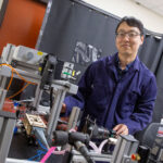
Electrical engineering Professor Trevor Thornton is leading a project through ASU’s AMPED Science and Technology Center to create transistors made of diamond and boron nitride

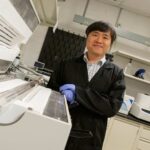
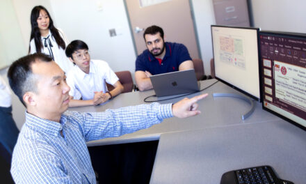
An artificial diamond being grown in a lab at Arizona State University. Trevor Thornton, a professor of electrical engineering in the Ira A. Fulton Schools of Engineering at ASU, is working with an interdisciplinary team of colleagues at ASU and Northrop Grumman Mission Systems to research the use of diamond and boron nitride in transistors. Photo courtesy of Franz Koeck/ASU
Silicon has long been the standard material for semiconductor devices. Power transistors, which are individual semiconductor switches that regulate the flow of electrical power, have traditionally been made with silicon, while more advanced modern transistors are made of silicon carbide or gallium nitride.
Trevor Thornton, a professor of electrical engineering in the School of Electrical, Computer and Energy Engineering, part of the Ira A. Fulton Schools of Engineering at Arizona State University, is leading a team researching the use of two new transistor materials: diamond and boron nitride.
Thornton’s team is conducting their research through ASU’s Advanced Materials, Processes, and Energy Devices Science and Technology Center, or AMPED STC. AMPED’s goal is to develop materials and technologies with industry partners to support the mission of Arizona’s New Economy Initiative.
The New Economy Initiative aims to improve Arizona’s competitiveness in developing advanced technology. AMPED specifically looks to develop technologies and materials used in the construction of batteries, solar electricity generation and power electronics, which convert electricity to a needed form when it’s moved through transmission channels.
The research team includes Thornton and other ASU faculty members including Terry Alford, a professor of materials science and engineering, Stephen Goodnick, a professor of electrical engineering, and Robert Nemanich, a Regents Professor of physics, as well as doctoral students in electrical engineering and materials science and engineering. They are working with Northrop Grumman Mission Systems as the industry partner for this project.
Diamond efficiency shines
Thornton explains that diamond is under investigation as a material for transistors because of its high thermal conductivity. Thermal conductivity refers to how well a material can dissipate heat.
He gives an analogy of a cool metal surface, which represents high thermal conductivity, and cotton, which represents low thermal conductivity.
“If you put your hand on a metal surface, the metal surface usually feels cool, whereas if you put your hand on a cotton duvet it immediately feels warm,” Thornton says. “That’s because the metal conducts heat away from your hand very quickly, and so your hand is being cooled, whereas the duvet is keeping your body heat in.”
Thornton says that diamond’s thermal conductivity is highly efficient compared to current materials. As one example, diamond’s thermal conductivity is eight to 10 times more efficient than gallium nitride. Harnessing diamond to its full potential could shrink the size of transistors by 90%.
Diamond also has a high breakdown field. This means that the material can handle a large amount of voltage relative to most materials before failure. A high breakdown field is ideal for applications that handle large amounts of power.
While diamond is the research team’s chosen material for the main body of a transistor, they are investigating the use of boron nitride, a chemical compound of boron and nitrogen, for the transistors’ electrical contacts.
Like diamond, boron nitride has a high breakdown field and high thermal conductivity. Goodnick’s portion of the research is primarily concerned with computer modeling and simulation of the use of boron nitride transistors.
The research team expects that by combining their knowledge of how diamond and boron nitride work as transistor materials, they can create transistors made from both materials. The team’s hope is that the materials complement each other and work even better together than individually.
“Ultra-wide bandgap semiconductor materials like diamond and boron nitride are expected to lead to more efficient energy conversion using less power with much smaller components,” Goodnick says. “This improves the future energy grid, which is essential for the ongoing transition toward renewable energy and electrification of the transportation sector.”
Better heat dissipation to improve communication
This research has applications that would be especially useful to communications technologies. Many satellites run on solar power, which requires transistors to turn the electricity into a form usable by the satellite.
“You can’t launch a power substation into space,” Thornton says. “Any improvement on size and weight in a satellite has a huge impact.”
Other communications technology the transistors could improve is a bit closer to home: cell phone towers. Transistors convert power to the proper form needed to produce radio frequency waves that cell phones use.
Thornton says that one of the biggest challenges faced when designing and operating cell phone towers is keeping them cool. This is especially the case in a hot environment like Phoenix.
The power transistors in older cell phone towers are typically made from silicon, while those in newer 5G systems will use gallium nitride. Thanks to its improved heat dissipation, Thornton’s team expects transistors made from diamond and boron nitride to greatly reduce the cooling power needed for cell towers. This makes the task of keeping cell towers from overheating far easier.
Shrinking substations
While the project with Northrop Grumman Mission Systems focuses on communications technology, transistors made from diamond and boron nitride also have applications in power conversion for electrical systems and for the electricity grid. These more efficient materials could reduce the size requirements for electricity grid substations.
Substations convert electricity into a usable form for homes and businesses. Typically, they take up an area of land the size of a building.
“If you wander around your neighborhood, sometimes there will be a big transformer surrounded by wires with signs warning you of death,” Thornton says. “That’s a substation. We’d like to make them smaller and more efficient.”
Nemanich, a faculty member in the ASU Department of Physics, leads a group conducting research on power electronics called the ULTRA Energy Frontier Research Center. He also leads a lab for growing artificial diamond material. These materials will be used by Thornton’s team in their research.
“We have been growing diamond for electronic devices for the last 10 years,” Nemanich says. “We believe our diamond deposition lab has unique capabilities for the development of electronic materials and devices.”
An interdisciplinary effort
In addition to Thornton’s electrical engineering expertise and Nemanich’s work with diamond as an electronic material, Alford, a faculty member in the School for Engineering of Matter, Transport and Energy, part of the Fulton Schools, provides his expertise on materials science.
Alford is working on materials characterization, or analyzing the properties of the materials the team is investigating. He also leads a part of the research looking into the use of new types of metallic electrical contacts connected to diamond as a substrate, and he co-advises a materials science and engineering doctoral student involved in the research with Thornton.
“I had done work on silicide, making electrical contacts on silicon, but I never worked on diamond,” Alford says. “I thought this would be a good opportunity to learn about diamond semiconductors.”
Working with Thornton’s team at the AMPED STC has given Alford the chance to conduct research that differs from his normal topics. He believes that his perspective as a materials scientist can help the team achieve its goals.
“I think we bring to the table a desire to understand the impact of a material’s defects,” Alford says. “We want to be able to understand those defects and how they impact a device’s performance.”
Looking to the future of electronics
The transistor research project is funded for two years through the AMPED STC partnership with Northrop Grumman Mission Systems. However, to fully realize the transistors’ potential for widespread applications, Thornton says it could take longer.
“We’ll have breakthroughs, but I don’t see it being widely adopted in the way we’re talking about for five to 10 years,” he says. “It’s that kind of medium- to long-term research of which some applications will happen quicker, while others will be 10 years for widespread consumer applications.”


